
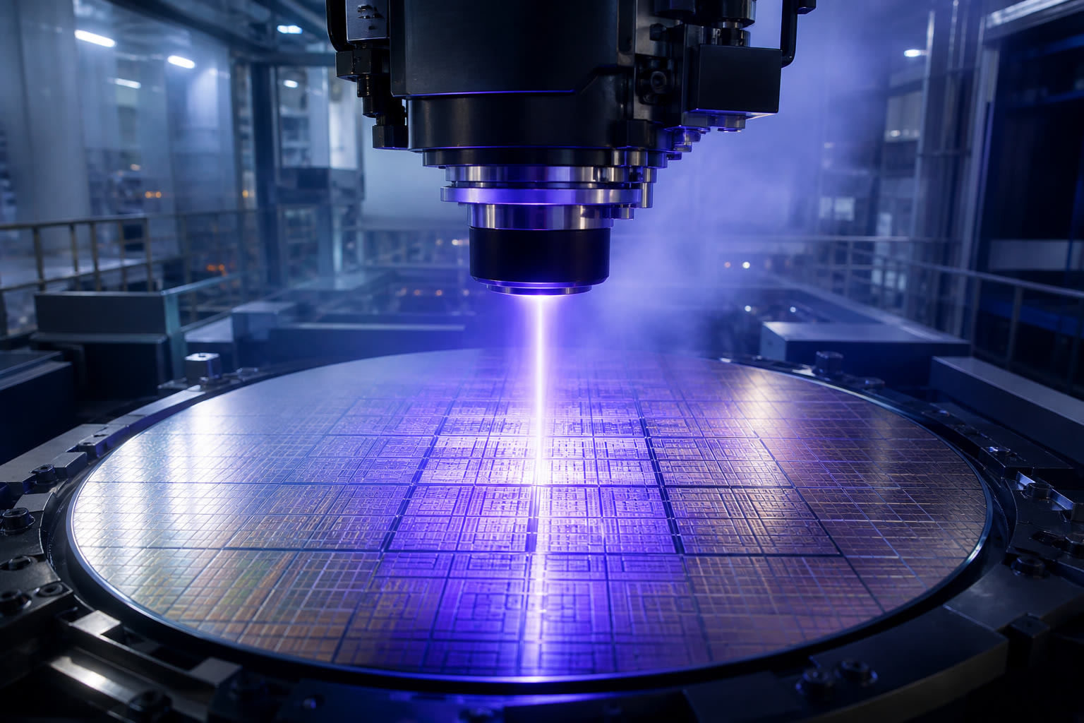
ASML said it will work with major chipmakers to move its newest High NA extreme-ultraviolet tools onto larger masks — so the machines that print finer features can also handle the giant data-center chips designed by Nvidia and others.
Today’s widely used EUV tools can print chips up to about 800 square millimeters. High NA tools can etch finer patterns but currently use a smaller mask, capping chip size. ASML plans a larger mask size so High NA can match today’s biggest accelerator footprints. CTO Marco Pieters told Reuters the industry move could lift those systems’ productivity by about 40% if it sticks.
Intel already uses High NA for laptop chips. TSMC said it plans High NA in advanced-node high-volume production from 2030; Samsung aims to bring High NA EUV into DRAM high-volume production by 2028. SK Hynix said it is evaluating the 12-inch-mask consortium and is targeting 2028 for High-NA EUV on DRAM. ASML plans a pilot line with the larger masks by 2031 and high-volume readiness by 2033.
Leave a Reply